| Previous Page | Print Page | Home |
This is for Tony Parks, KB9YIG, who has developed this little device. Thanks
Tony for great support at all times!
Nov. 15th, 2006
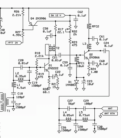
I have received a beta kit of the SoftRock V6.0 RxTx from Tony Parks KB9YIG. For details see http://groups.yahoo.com/group/softrock40 . As the design being beta had not been completely verified, I decided to build it up block by block and do tests in between. Clock generator and Rx worked fine at once. The Tx modulator also worked fine after tweaking the OpAmps a little bit with pull-up resistors. With the Tx I encountered severe problems, though. Below you can see the schematic of the original Tx section.
After not even getting close to 0.4 W output power I tested the PA transistor (Q2, 2N3866) off board and found it ok for DC but defective for RF in a test circuit similar to the final PA stage. I replaced it with a 2N3553. In order to set the collector current of Q2 to highest linearity, I had to add 100 Ohms in series with D1. Besides this I had implemented the official changes published on the Yahoo board (RFC1 replaced by 100 Ohms, modified low pass filter with the values published on the board). As the PA still appeared to work on the limit I decided to do a complete analysis.
On the following picture you see the measured frequency response of the isolated Tx low pass filter:
It shows a fair match to 50 Ohms and moderate attenuation of 0.9 dB at 7 MHz. It has to be kept in mind though, that 0.9dB means 20% less output power (100 mW loss). So a little rework might pay off here.
As I made bad experiences in the past with low Q capacitors I decided to measure the impedance of one 1.5nF capacitor. The result can be seen in the next image.
This is a perfect capacitor! There is no degradation to the filters to be expected.
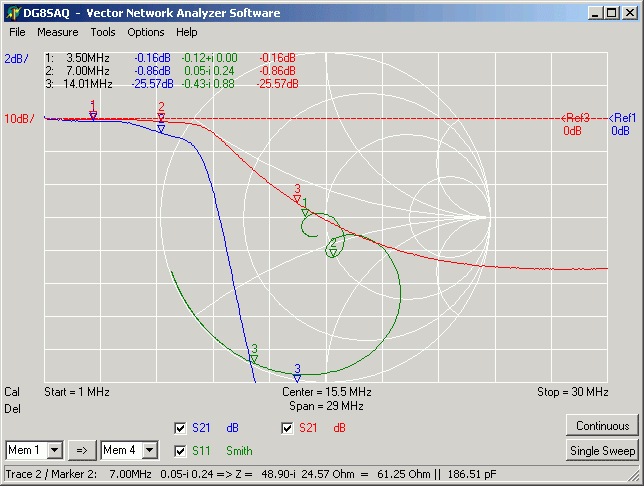
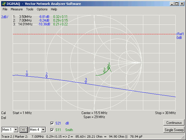
Next I measured the isolated final PA stage without low pass filter.
I added a 30 dB coaxial pad to the output in order to not overload the network analyzer. So 1.3 dB gain at 7 MHz actually means 31.3 dB gain. This is a small signal gain, though. I have also measured the gain at 7 MHz at 0.5 W output with signal generator and scope to be 27 dB. It is to be noted that the input impedance is rather low and capacitive (15 Ohms || 1.2 nF @ 7MHz).
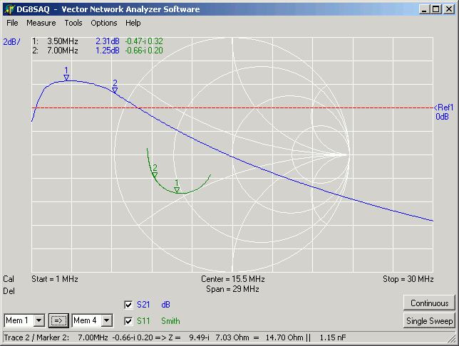
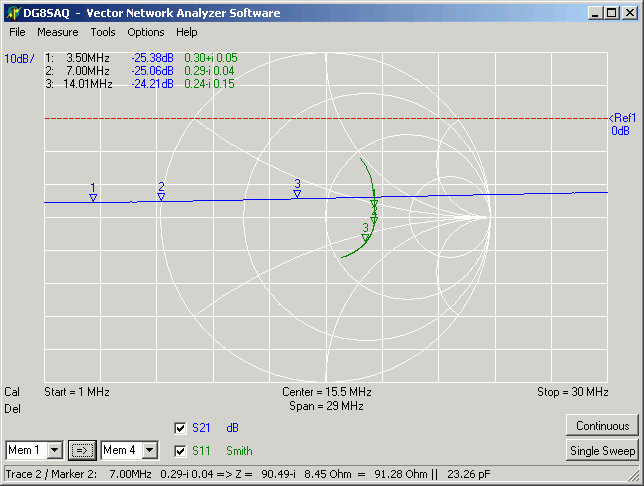
Next section backwards is the driver stage Q1. Here's its frequency response:
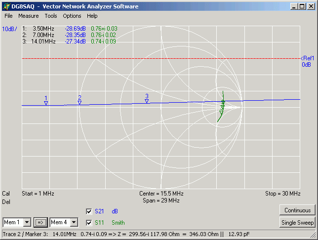
Here again I used a 30 dB pad on output. So -10dB "gain" actually means 20 dB gain of the stage. Note that the input impedance is rather high and capacitive ( 95 Ohms || 78 pF @ 7 MHz). In order to test if the driver is well power matched to the final stage I measured the driver in reverse direction. Here's the result this time without 30 dB pad:
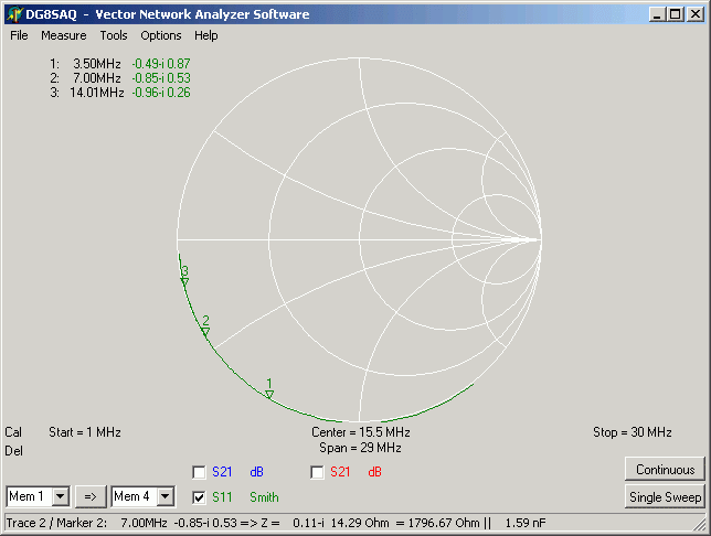
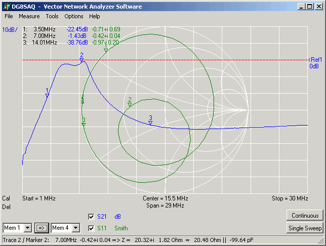
The output impedance (denoted with S11 here) of the driver is also rather high and capacitive ( 91 Ohms || 23 pF @ 7 MHz). So considerable mismatching losses are to be expected. To test if the output balun is doing its job correctly, I did the same measurement straight into the collector of Q1:
The output impedance has risen by a factor of 4 as is to be expected for a 4:1 transformer. Maybe an impedance transformation ratio of 16:1 would be more appropriate for T2.
Finally I measured the transfer function of the isolated input band pass filter. The network analyzer signal was fed into the secondary winding of T1. The signal was detected at the hot end of T2. Here is the result
The filter shows a reasonable attenuation at 7 MHz of 1.4 dB. Apparently it is not designed to operate in a 50 Ohms system, but it works nicely also in mismatched condition.
Finally, I connected all blocks of the Tx chain together to measure the uncompressed achievable output power.
As the low pass filter blocks all harmonics, compression cannot be measured with a single tone signal. At least two frequencies are necessary to see the effects of compression. I generated such a Tx signal by applying a 1 kHz sinewave to ONE audio input only of the IQ Tx modulator, the other input was grounded. With this input signal the PA output looked like this:
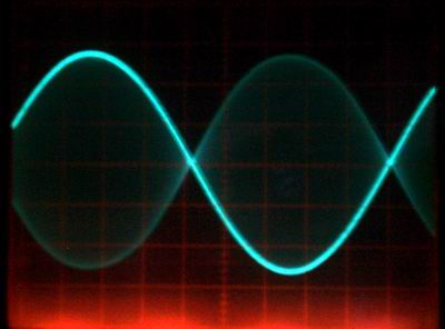
One can see a dual sideband signal with suppressed carrier. I overlayed the input sinewave on the second scope channel so I could check if the envelope of the RF is identical with the input signal. If so, the PA operates linearly. The above scope image was taken with 2 V/div for the RF signal. So the peak output power calculates to be 0.3 W. Increasing the audio input signal without changing the scope settings yields the following image:
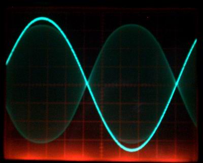
Peak output power is 0.4 W but compression can clearly be seen, i.e. the RF amplitude doesn't follow the audio signal for large amplitudes but stays below.
I also determined the efficiency factor of the final PA stage. The DC collector current of Q2 can easily be measured by measuring the dc voltage at the emitter. A voltage of 0.19 V in my case calculates to a current of 190 mA thru R24. The average DC voltage at the collector is 12V-0.7V=11.3V. So 0.19A*11.3V=2.15W heat is produced in Q2 ( I decided to add a cooling star to Q2). Output power was 0.5W in this case. So the efficiency of the final stage is 0.5/2.15=23%.
| Previous Page | Print Page | Home |